Κατέβασμα παρουσίασης
Η παρουσίαση φορτώνεται. Παρακαλείστε να περιμένετε

1
Τεχνικές διαμόρφωσης της επιφάνειας ηλιακών κυττάρων Surface Texturing Optical Lithography + Etching Alkaline or Acidic Etching Mechanical V-Grooving Laser Surface Texturing

2
Ανισοτροπική υγρή χημική εγχάραξη κρυσταλλικού πυριτίου. Scanning electron micrographs of an oriented silicon substrate after immersion in an anisotropic wet chemical etchant.

3
Διαμόρφωση της επιφάνειας ηλιακού κυττάρου με την κατασκευή V shaped microgrooves.

4
Διαμόρφωση της επιφάνειας ηλιακού κυττάρου με ανάστροφες πυραμίδες.

5
Διαμόρφωση της επιφάνειας ενός κυττάρου πυριτίου για την αποτελεσματικότερη παγίδευση των φωτονίων της προσπίπτουσας ηλιακής ακτινοβολίας. Light trapping properties of pyramidally textured surfacesLight trapping properties of pyramidally textured surfaces. Campbell PCampbell P, Green MA.Green MA Journal of Applied Physics, 1987, 62(1), 243. High performance light trapping textures for monocrystalline silicon solar cellsHigh performance light trapping textures for monocrystalline silicon solar cells. Campbell PCampbell P, Green MA.Green MA Solar Energy Materials and Solar Cells, 2001, 65(1-4), 369 – 375.
, 243. High performance light trapping textures for monocrystalline silicon solar cellsHigh performance light trapping textures for monocrystalline silicon solar cells. Campbell PCampbell P, Green MA.Green MA Solar Energy Materials and Solar Cells, 2001, 65(1-4), 369 –")
6
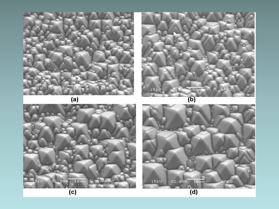
Scanning electron microscope photograph οf a textured silicon surface. Texture etching of silicon : method. Bailey WL Bailey WL, Coleman MG, Harris CB, Lesk IA.Coleman MGHarris CBLesk IA United States Patent: 4137123. Scanning electron microscope photograph of a textured silicon surface. Image Courtesy of The School of Photovoltaic & Renewable Energy Engineering, University of New South Wales.

7
Alkaline Etching of Silicon Surfaces NaOH (2 Wt%) / IPA (6 wt%) / DIH 2 O Temperature : 82 0 C Etching times : 25, 30, 35 and 40 minutes respectively Average height of pyramids : ~3, 5, 7 and 10 micrometers approximately Fabrication of Crystalline Silicon Solar Cell with Emitter Diffusion, SiNx Surface Passivation and Screen Printing of Electrode. S. M. Iftiquar 1, Youngwoo Lee 1, Minkyu Ju 1, Nagarajan Balaji 2, Suresh Kumar Dhungel 1 and Junsin Yi 1, 2 [1] College of Information and Communication Engineering, Sungkyunkwan University, Republic of Korea [2] Department of Energy Science, Sungkyunkwan University, Republic of Korea

9
Διαμόρφωση της επιφάνειας ηλιακού κυττάρου πυριτίου – Laser texturing The hills and valleys of the nanospikes increase the surface area and reduce the reflection of light. The heights of nanospikes range from 10 to 100 millionths of a meter. Τhis laser texturing process was developed by Professor Mool C. Gupta of the Department of Electrical and Computer Engineering of the University of Virginia. It was patented through the University of Virginia Patent Foundation.

10
Surface texturing of Si solar cells by mechanical fabrication of V-grooves Latest results on semitransparent POWER silicon solar cells Arnd Boueke, Ralph Kuhn, Peter Fath, Gerhard Willeke, Ernst Bucher Solar Energy Materials and Solar Cells 65 (2001) 549-553
")
11
Lasers in Photovoltaics Silicon Surface Texturing using Laser Beams Laser Edge Isolation Scribing Emitter Wrap Through (EWT) Si Solar Cells using Laser Drilling Metal Wrap Through (MWT) Si solar Cells using Laser Trepaning Fabrication of Semi-transparent Si Solar Cells using Laser Cutting
 Si Solar Cells using Laser Drilling Metal Wrap Through (MWT) Si solar Cells using Laser Trepaning Fabrication of Semi-transparent Si Solar Cells using Laser Cutting")
12
Ημιδιαφανή Ηλιακά Κύτταρα Πυριτίου Εργαστήριο Ηλεκτρονικών Υλικών Τμήμα Μηχανικών Επιστήμης Υλικών Πανεπιστήμιο Ιωαννίνων

13
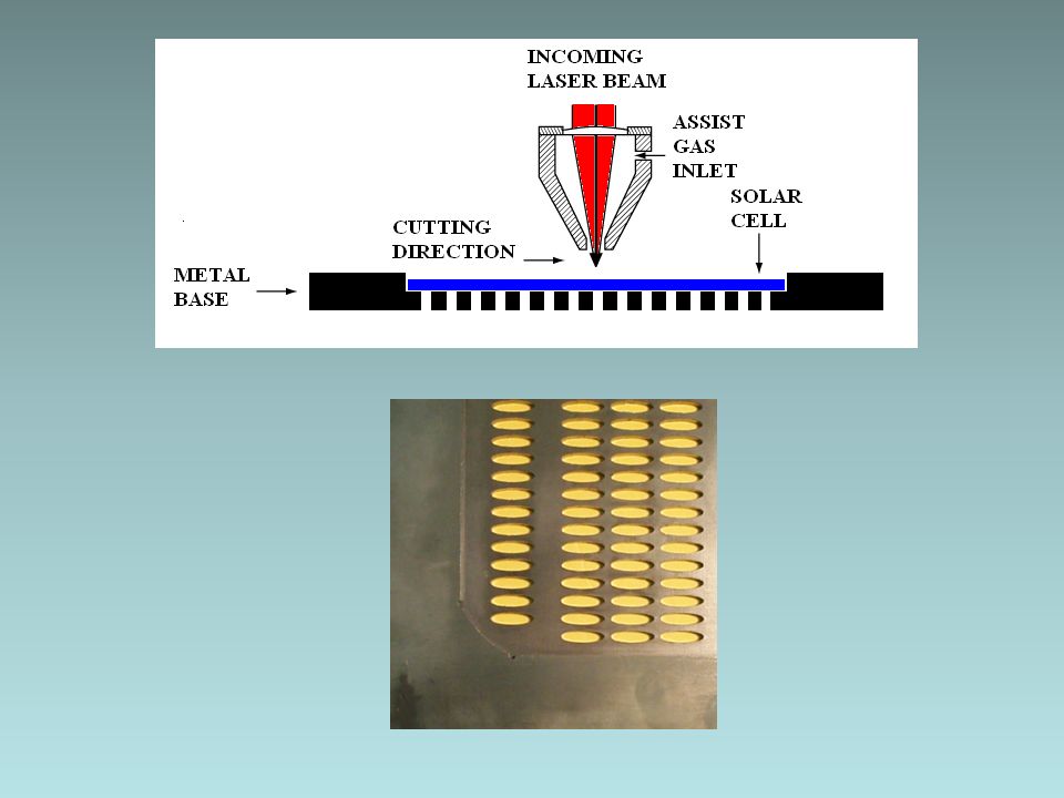
Μεταλλική βάση ειδικά σχεδιασμένη για την κατασκευή, με τη χρησιμοποίηση δέσμης laser, ημιδιαφανών ηλιακών κυττάρων πυριτίου.

15
Χαρακτηριστικές καμπύλες α) ηλεκτρικού ρεύματος – διαφοράς δυναμικού (I-V) και β) ισχύος – διαφοράς δυναμικού (P-V) ημιδιαφανών ηλιακών κυττάρων πυριτίου.
 ηλεκτρικού ρεύματος – διαφοράς δυναμικού (I-V) και β) ισχύος – διαφοράς δυναμικού (P-V) ημιδιαφανών ηλιακών κυττάρων πυριτίου.")
16
Χαρακτηριστικές καμπύλες α) ηλεκτρικού ρεύματος – διαφοράς δυναμικού (I-V) και β) ισχύος – διαφοράς δυναμικού (P-V) ημιδιαφανών ηλιακών κυττάρων πυριτίου. Ηλιακά κύτταρα με μεγάλο αριθμό ελλείψεων. Οι κοπές έγιναν στις εγκαταστάσεις της εταιρείας Μεταλλεμπορική Α.Ε. στη βιομηχανική περιοχή της Πάτρας.

17
Διαφορετικές τεχνικές κατασκευής ηλιακών κυττάρων πυριτίου Standard monocrystalline Si solar cells Emitter wrap-through (EWT) Si solar cells Metal wrap-through (MWT) Si solar cells
 Si solar cells Metal wrap-through (MWT) Si solar cells")
18
Semi-insulating InP substrate – Fe-doped – 400 μm In 0.52 Al 0.48 As buffer layer – un-doped - 200 μm In 0.53 Ga 0.47 As – quantum well – 30 nm – N 2DES ~ 3 x 10 12 cm -2 - - - - - - - - - - - - - - - - - - - In 0.52 Al 0.48 As – spacer layer – un-doped – 5 nm + + + + + + + + + + + + + + + In 0.52 Al 0.48 As – Schottky layer – un-doped - 20 nm Si δ-doped layer – N D ~ 5x10 12 cm -2 In 0.53 Ga 0.47 As – Si-doped cap layer – 7 nm – N D ~ 3x10 18 cm -3

19
Semi-insulating InP substrate – Fe-doped – 400 μm In 0.52 Al 0.48 As buffer layer – undoped - 200 μm In 0.53 Ga 0.47 As – quantum well – 30 nm – N 2DES ~ 3 x 10 12 cm -2 - - - - - - - - - - - - - - - - - - - In 0.52 Al 0.48 As – spacer layer – undoped – 5 nm + + + + + + + + + + + + + + + In 0.52 Al 0.48 As – Schottky layer – un-doped - 20 nm Si δ-doped layer – N D ~ 5x10 12 cm -2 In 0.53 Ga 0.47 As - Si doped

20
Semi-insulating InP substrate – Fe-doped – 400 μm In 0.52 Al 0.48 As buffer layer – undoped - 200 μm In 0.53 Ga 0.47 As – quantum well – 30 nm – N 2DES ~ 3 x 10 12 cm -2 - - - - - - - - - - - - - - - - - - - In 0.52 Al 0.48 As – spacer layer – undoped – 5 nm + + + + + + + + + + + + + + + In 0.52 Al 0.48 As – Schottky layer – un-doped - 20 nm Si δ-doped layer – N D ~ 5x10 12 cm -2 In 0.53 Ga 0.47 As – Si-doped Ohmic contact – Ni/Ge/Au T-gate

21
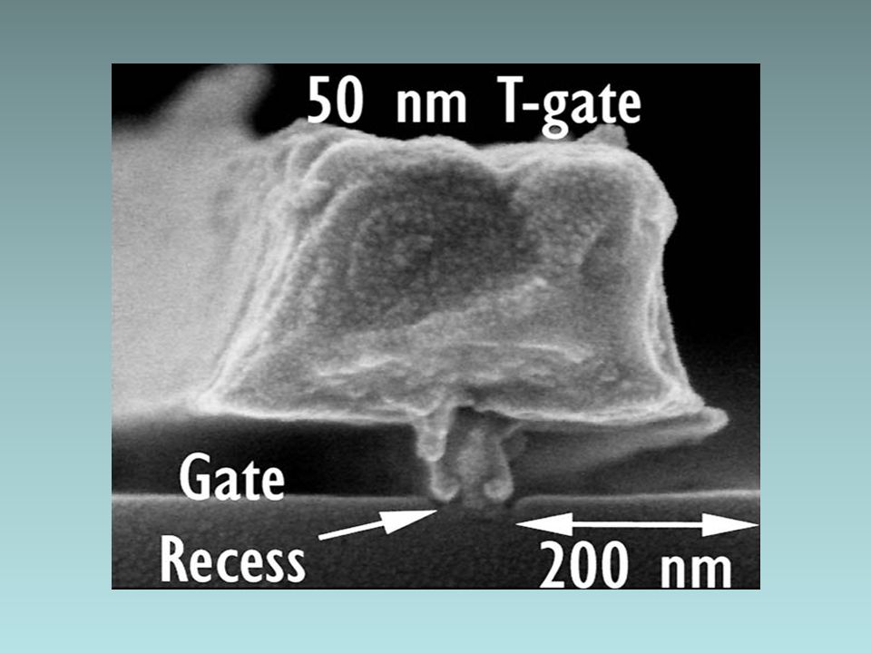
Resist development prior to T-gate metal deposition

23
T-gates for high frequency III-V transistors

Παρόμοιες παρουσιάσεις


 ωφελέειν ή μη βλάπτειν ωφελέειν = θεραπευτική παρέμβαση μη βλάπτειν = ασφάλεια ασθενών.>")


 μηρυκαστικά,>")


